- 您现在的位置:买卖IC网 > Sheet目录3873 > PIC16F627-04/P (Microchip Technology)IC MCU FLASH 1KX14 COMP 18DIP
2003 Microchip Technology Inc.
Preliminary
DS40300C-page 13
PIC16F62X
3.0
MEMORY ORGANIZATION
3.1
Program Memory Organization
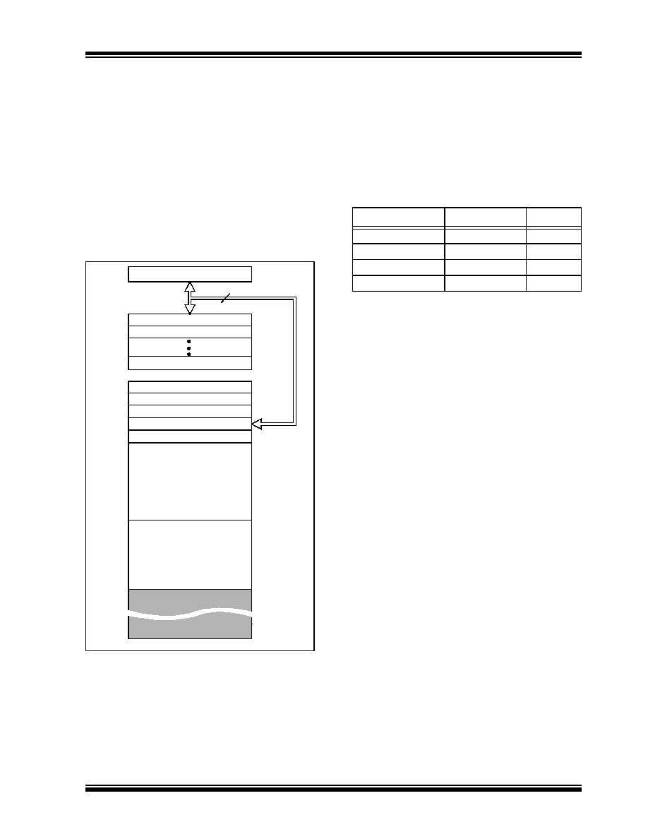
The PIC16F62X has a 13-bit program counter capable
of addressing an 8K x 14 program memory space. Only
the first 1K x 14 (0000h - 03FFh) for the PIC16F627
and 2K x 14 (0000h - 07FFh) for the PIC16F628 are
physically implemented. Accessing a location above
these boundaries will cause a wrap-around within the
first 1K x 14 space (PIC16F627) or 2K x 14 space
(PIC16F628). The RESET vector is at 0000h and the
interrupt vector is at 0004h (Figure 3-1).
FIGURE 3-1:
PROGRAM MEMORY MAP
AND STACK
3.2
Data Memory Organization
The data memory (Figure 3-2) is partitioned into four
banks, which contain the general purpose registers and
the Special Function Registers (SFR). The SFR’s are
located in the first 32 locations of each Bank. Register
locations 20-7Fh, A0h-FFh, 120h-14Fh, 170h-17Fh
and
1F0h-1FFh
are
general
purpose
registers
implemented as static RAM.
The Table below lists how to access the four banks of
registers:
Addresses F0h-FFh, 170h-17Fh and 1F0h-1FFh are
implemented as common RAM and mapped back to
addresses 70h-7Fh.
3.2.1
GENERAL PURPOSE REGISTER
FILE
The register file is organized as 224 x 8 in the
PIC16F62X. Each is accessed either directly or
indirectly through the File Select Register FSR (See
PC<12:0>
13
000h
0004
0005
03FFh
1FFFh
Stack Level 1
Stack Level 8
RESET Vector
Interrupt Vector
On-chip Program
Memory
CALL, RETURN
RETFIE, RETLW
Stack Level 2
07FFh
PIC16F627 and
PIC16F628
PIC16F628 only
On-chip Program
Memory
RP1
RP0
Bank0
00
Bank1
01
Bank2
10
Bank3
11
发布紧急采购,3分钟左右您将得到回复。
相关PDF资料
PIC18F45J10-I/ML
IC PIC MCU FLASH 16KX16 44QFN
PIC18F24K22-I/ML
IC PIC MCU 16KB FLASH 28QFN
PIC16CR76-I/SS
IC PIC MCU 8KX14 28SSOP
PIC16F887-I/P
IC PIC MCU FLASH 8KX14 40DIP
PIC16CR76-I/SP
IC PIC MCU 8KX14 28DIP
PIC16CR76-I/SO
IC PIC MCU 8KX14 28SOIC
PIC16CR76-I/ML
IC PIC MCU 8KX14 28QFN
PIC16CR74T-I/ML
IC PIC MCU 4KX14 44QFN
相关代理商/技术参数
PIC16F627-04/P
制造商:Microchip Technology Inc 功能描述:IC 8BIT FLASH MCU 16F627 DIP18
PIC16F627-04/SO
功能描述:8位微控制器 -MCU 1.75KB 224 RAM 16I/O 4MHz SOIC18 RoHS:否 制造商:Silicon Labs 核心:8051 处理器系列:C8051F39x 数据总线宽度:8 bit 最大时钟频率:50 MHz 程序存储器大小:16 KB 数据 RAM 大小:1 KB 片上 ADC:Yes 工作电源电压:1.8 V to 3.6 V 工作温度范围:- 40 C to + 105 C 封装 / 箱体:QFN-20 安装风格:SMD/SMT
PIC16F627-04/SO
制造商:Microchip Technology Inc 功能描述:8BIT FLASH MCU SMD 16F627 SOIC18
PIC16F627-04/SO
制造商:Microchip Technology Inc 功能描述:Microcontroller IC Number of I/Os:16
PIC16F627-04/SS
功能描述:8位微控制器 -MCU 1.75KB 224 RAM 16I/O 4MHz SSOP20 RoHS:否 制造商:Silicon Labs 核心:8051 处理器系列:C8051F39x 数据总线宽度:8 bit 最大时钟频率:50 MHz 程序存储器大小:16 KB 数据 RAM 大小:1 KB 片上 ADC:Yes 工作电源电压:1.8 V to 3.6 V 工作温度范围:- 40 C to + 105 C 封装 / 箱体:QFN-20 安装风格:SMD/SMT
PIC16F627-04E/P
功能描述:8位微控制器 -MCU 1.75KB 224 RAM 16I/O RoHS:否 制造商:Silicon Labs 核心:8051 处理器系列:C8051F39x 数据总线宽度:8 bit 最大时钟频率:50 MHz 程序存储器大小:16 KB 数据 RAM 大小:1 KB 片上 ADC:Yes 工作电源电压:1.8 V to 3.6 V 工作温度范围:- 40 C to + 105 C 封装 / 箱体:QFN-20 安装风格:SMD/SMT
PIC16F627-04E/SO
功能描述:8位微控制器 -MCU 1.75KB 224 RAM 16I/O 4MHz Ext Temp SOIC18 RoHS:否 制造商:Silicon Labs 核心:8051 处理器系列:C8051F39x 数据总线宽度:8 bit 最大时钟频率:50 MHz 程序存储器大小:16 KB 数据 RAM 大小:1 KB 片上 ADC:Yes 工作电源电压:1.8 V to 3.6 V 工作温度范围:- 40 C to + 105 C 封装 / 箱体:QFN-20 安装风格:SMD/SMT
PIC16F627-04E/SS
功能描述:8位微控制器 -MCU 1.75KB 224 RAM 16I/O 4MHz Ext Temp SSOP20 RoHS:否 制造商:Silicon Labs 核心:8051 处理器系列:C8051F39x 数据总线宽度:8 bit 最大时钟频率:50 MHz 程序存储器大小:16 KB 数据 RAM 大小:1 KB 片上 ADC:Yes 工作电源电压:1.8 V to 3.6 V 工作温度范围:- 40 C to + 105 C 封装 / 箱体:QFN-20 安装风格:SMD/SMT